Saturday, September 11, 2010

FLYBACK CALCULATIONS - PART VIII

The following figures are for a flyback AC-DC converter that was designed as a demo circuit for purposes of showing circuit analysis and simulation. The design is not intended to be suitable for use as an actual production converter and it would not necessarily meet requirements for agencies such as UL or other testing and certification agencies. As shown in Fig. the converter appears to have a secondary side isolated from the primary but in the actual simulations both primary and secondary are connected to the SPICE zero or ground node to simplify simulation convergence. The figures shown in order of appearance are first the overall loop gain versus frequency, the control-to-output gain versus frequency, and the simulation schematic for the converter design. Click on the figures for a larger view.


Fig. 1 shows a so-called universal input AC-DC converter. The converter design shown is supposed converter AC 50-60 HZ, 90 to 265 VAC input to a 5 volt output at 1 amp. The switching frequency is approximately 100KHZ. The circuit shown is an actual simulation schematic which shows that the circuit will operate as desired and is stable with a load transient from a minimum load of 10 MA to 1AMP as is shown in the simulation result diagram below Fig. 1. Click on the figures for a larger view.

In the design we have used the principles discussed in our previous posts but it should be noted that in some cases component values are adjusted to give improved simulation results (The converter has different specifications than the examples in previous posts.)

The main purpose of this post is to review the feedback circuit calculations.

The converter is a current mode control type that operates in discontinuous current mode throughout its operating range.

The current control factor is

K = Ilim / Vfbsat = 1 / 5.8 = 0.172

The zero in the control-to-output gain is

wz = 1 / ( Rc * Co ) = 1 / ( 0.09 * 6.8 *10^-4 ) = 16340 radians or 2600HZ

Next, we compute the worst case control-to-output gain response pole at minimum load (maximum resistance load)

wp = 2 / ( RLmax * Co ) = 2 / ( 500 * 6.8 * 10^-4 ) = 5.882 radians or approx 1HZ.

To make our equations a little easier to type here let me make the following substitutions:

Z1 = 1 + ( S / wz ) where S is the complex operator = j * 2 * Pi * f (using only the imaginary component of S in this work.)

P1 = 1 + ( S / wp )

The values of Z1 and P1 are only dummy variables and not actual frequencies, but their values will be different at different frequencies. Also note here that because we always operate in discontinuous current mode (DCM), we do not have to worry about a right-half plane zero which would otherwise be present if we were operating in continuous current mode (CCM.)

We can now type a simple equation for the control-to-output gain as a function of frequency as follows:

Gco = ( Vo / VFB ) * ( Z1 / P1 )

where Vo is the nominal output voltage ( 5 volts ) and VFB is the nominal feedback voltage ( 2.5 volts .) A plot of the control-to-output gain is shown in the post.

Next we have a simple compensation network that is similar to the ones used in most flyback converters of this type. The purpose of the compensation network is to make the system stable with a reasonable control band-width and known feedback characteristics, such as cross-over frequency, phase and gain margins.

First we compute the constant gain factor K as

K = RB / ( R1 * RD * CF ) = 1000 / ( 5360 * 100 * 1 * 10^-6 ) = 1866

where RB is the PWM controller IC feedback input impedance (we added a 1K to ground at the ouput of opto-coupler to establish a known value for this quantity.) RD is the feedback amplifier IC collector resistance, and CF is the compensation capacitance for this amplifier.

We need to have a compensation zero to help cancel the converter pole at 1 HZ. But the compensation pole will be set at approximately 15HZ:

wzc = 1 / ( ( RF + R1 ) * CF ) = 1 / ( ( 5100 + 5360 ) * 1 *10^-6 ) = 95.6 radians
or 15.2 HZ.

Also we need to set a compensation pole. We will set this pole at a relatively high frequency in order to flatten over-all loop gain and establish reasonable bandwidth.

wpc = 1 / ( RB * CB ) = 1 / ( 1000 * 1 * 10^-8 ) = 100000 radians

or 15920 HZ ( still well below the switching frequency of 100KHZ.)

Now for convenience in typing the compensation equation we will set some dummy variables as

Zc = 1 + ( S / wzc )

and

Pc = 1 + ( 1 / wpc )

We can now write a simple equation for the compensation gain as a function of frequency as

Gc = - ( K / S ) * ( Zc / Pc )

In the above equation we note that the negative sign is because we are using negative feedback in the compensation circuit to control the converter.

Now it is known that the overall loop gain, that is the gain of the converter from its input around to the feedback input at the IC controller can be computed from the product of the control-to-output gain and the compensation gain as

Gol = Gco * Gc

The results of the calculation vs. frequency is shown in the chart for the loop gain. The calculations can be done by math programs such as Mathcad, etc.

You will note that the loop gain has a cross-over frequency of approximately 40HZ (which could probably be improved a lot with some improvements to the compensation circuit.) The loop gain at DC is pretty good at over 50DB and the cross-over slope is -20db per decade indicating absolute stability (this is also verified by SPICE simulation of the closed loop circuit of Fig. 1.) The phase shift is a little over 70 degrees at crossover which gives us a phase margin of 110 degrees which also indicates absolute stability. So this converter is a relatively low bandwidth design but should be very stable over all operating conditions that wre within its specifications. The fact that it operates in DCM also helps simplify stabilization, but this is not to say that we should always operate in DCM. In fact, if the converter had been designed as a CCM type, it would be capable of more power and peak ripple current in the output filter capacitor could be reduced.

Saturday, September 4, 2010

FLYBACK CALCULATIONS - PART VII


In this section we will discuss the snubber network for the transistor switch on the primary side of the converter (see Fig.1. Click on the figure to see a larger view.) First an estimate is made for the voltage spike that is to be snubbed as 2.5 times the reflected voltage from the secondary as

Vsn = 2.5 * VRO

With VRO previously determined to be 350 volts (see previous posts), we have

Vsn = 875 volts

Next we use this estimate to calculate an approximate value for the power dissipated in the snubber network.

Psn = 0.5 * Fs * Llk * Idspeak^2 * Vsn / (Vsn -VRO)

where Fs is the switching frequency, Llk is the transformer leakage inductance, and Idspeak is the peak transistor switch current. Our calculation results in

Psn = 0.316 watts

where the data we used is from our design example as

Fs = 100KHZ
Llk = 141 microhenry
Idspeak = 0.164

Now we can calculate a rough estimate of what the snubber resistor value should be (usually it is necessary to change the value based on actual snubber network performance but it gives us a starting point.)

Rsn = Vsn^2 / Psn = 2.4 megohm

(In the actual design, this resistor was changed to 360K.)

Using the 2.4 megohm value for the snubber resistor we will calculate the ripple voltage on the capacitor we have


dVsn = Vsn / ( Csn * Rsn * Fs ) = 3.6 volts

with Csn set to 0.001 microfarad. Note that if the value of Csn is set too hihg the operation of the flyback converter will not work well, e.g., values above 0.01 microfarad usually do not provide good results depending on the other values used in the design such as the primary inductance value. Remember that the primary inductance and the snubber capacitor form a "tank" circuit that can resonate and this is not usually desirable in a standard flyback converter.

We now have a preliminary design for the snubber network.

Friday, August 27, 2010

FLYBACK CALCULATIONS - PART VI


In this part we will calculate the RMS current ripple in the main output filter capacitor.

First we need to calculate the main output secondary current using the following data:

Idrms = 0.2 A
Dmax = 0.85
VRO = 350 volts
KL = 1.0
VF1 = 1.0 volt
Vo1 = 14 volts

where Idrms is the rms transistor switch current, Dmax is the maximum allowable duty cycle (usually limited by the main PWM control IC), VRO is the secondary voltage reflected to the primary side, Vo1 is the nominal output voltage, VF1 is the forward voltage of the output diode, and KL is the load occupying factor for the main output (1.0 if there is only one output winding.)

The equation for the secondary RMS current is

Isecrms = Idsrms * (((1 - Dmax) / Dmax )^0.5) * VRO * KL / (Vo1 + VF1)

Isecrms = 1.96 A

The output current Io is specified as 0.3 amps, so now we can calculate the output capacitor ripple current. This current is usually inconveniently large for flyback converters and cheap converters are sometimes found to have an output filter capacitor that is under-rated for ripple current. The risk is that the capacitor will overheat, dry-out too fast and the converter will fail to operate as intended. The ripple current is calculated as follows:


Icaprms = ( Isecrms^2 - Io^2 )^0.5

Icaprms = 2.28 A

Note that a continuous current mode (CCM) converter will have a lower secondary RMS current for a given output current load.

So we will need to have a capacitor that is rated at 2.3 amps or better for this design. It is better to use one large capacitor instead of smaller capacitors in parallel to meet the current requirement as parallel capacitors will not necessarily share ripple current equally and one or more of them could overheat. It is usually good though to put small capacitors in parallel such as ceramic chip caps for filtering high frequency noise.

Assume that we have the additional data as follows:


Co = 330UFD

Rc = 0.07 ohm

Idspeak = 0.3 A

Fs = 100KHZ

where Co is the output filter capacitance total, Rc is the equivalent series resistance of the capacitance, Idspeak is the peak transistor switch current, and Fs is the converter switching frequency.

Now we can calculate the theoretical output ripple or noise voltage using the equation

dVo1 = Io * Dmax / (Co * Fs ) + Idspeak * VRO * Rc * KL / (Vo1 + VF1 )

dVo1 = 0.498 volts

On an output voltage of 14 volts, 0.498 volts is about 3.6%. This value is probably OK for a battery charger converter, but probably too high if the voltage is to be used to power some electronic circuit. For a lower output ripple voltage, it would be necessary to increase capacitance value, reduce the equivalent series resistance of the capacitor, or both. Notice that the above calculation ignores the effects of the capacitor series inductance and the inductance of the circuit wires or circuit board traces. A low inductance layout is very important to keep noise low.

Wednesday, August 18, 2010

AC-DC FLYBACK CALCULATIONS - PART V


One of the most important things to determine on the AC-DC flyback converter are the RMS secondary winding currents. The RMS current must be filtered by a capacitor which is usually an aluminum electrolytic capacitor or some type of large capacitance high ripple current capable capacitor. One of the main failure modes of poorly designed flyback converters is an inadequate current rating for the filter capacitors. If the output capacitor is over-stressed with ripple current beyond its ratings it will run hot, dry out if it is a wet electrolytic, and otherwise fail casuing converter failure.

We can calculate the RMS current for each secondary winding according to a simple formula as follows:

Isecrms = Idsrms * (( 1 - Dmax ) / Dmax )^0.5 * VRO * KL / ( Vo1 + Vf1 )

where we have previously calculated the rms switch current Idsrms = 0.234 A, VRO = 349 volts, and we have specified Vo1 = 14 volts, Vf1 = 1 volts, and the load occupying factor KL has been set to 0.8 or 80% of the total load on the Vo1 output.

The answer is then that Isecrms = 1.8 amps. This is not a trival amount of ripple current to deal with and it will require a large electroylitic capacitor or several capacitors in parallel to handle the current. Note that it is difficult to parallel capaciotrs to handle the total load because one capacitor will more than likely try to handle most of the load and overheat while the other ones are not handling their share.

Another thing to be concerned about in flyback converters is the rating of the diode that feeds current to the filter capacitor from the secondary winding (see Fig. 1 -click on the figure for a larger view.) The current rating of the diode must be able to handle the RMS current we just calculated above and it must have a high enough voltage rating to handle the reverse spikes which are present on every switch cycle of the converter. We can calculate the reverse voltage on the diode from the following formula:

Vdr = Vo1 + Vdcmax * ( Vo1 + Vf1 ) / VRO

where Vo1 is the output DC voltage, 14V, Vdcmax is the max input voltage, 1000V,
Vf1 is the forward diode voltage, 1 volt, and VRO is the voltage reflected from secondary to primary on each switch cycle, 349 volts.

Vdr = 56.9 volts

is the peak reverse voltage on the diode.

It is customary to comput the VRRM (the voltage rating reverse maximum value) as

VRRM = 1.3 * Vdr = 74 volts

The VRRM value we computed is beyond the normal max for schottky diodes of 45 volts but there are some hybrid schottkys that will rate higher. The advantage of schottky diodes is that they have a lower forward voltage drop and therefor dissipate less heat and power for a given current load. If the output voltage had been 5 volts instead of 14, we could then have used a 35V or 45V schottky diode as VRRM would have calculated to 29 volts.

Thursday, August 12, 2010

FLYBACK CALCULATIONS - PART IV


In all switchmode converters that use a high frequency switching inductor or transformer, such as the typical AC-DC flyback converter shown if Fig. 1, it is of critical importance to avoid saturation of the inductor or transformer. If saturation occurs, the inductance of the transformer or inductor will decrease greatly so that the windings will no longer support the applied voltage. If saturation occurs when the transistor switch is in the on-state, the switch current is theoretically unlimited and this could lead to destruction of the converter. Even when current mode control is used, the initial turn-on spike will be so large that it most likely will cause the switch to fail.

To avoid going into saturation, the transformer must be designed so that at maximum current (set by the current limit), the transformer or inductor will not saturate. Therefore we need to determine the maximum magnetic field density (flux density) that the transformer core material will support (carefully the core manufacturer's data sheet), the effective cross-sectional area of the core, the inductance of the inductor or the primary of the transformer, and the maximum current set by the current limit. Then we must calculate the minimum number of inductor or primary turns that will be required to avoid saturation. The number of turns required is directly proportional to the product of the inductance and the maximum current and inversely proportional to the product of the maximum flux density and the core area.

Npmin = Lm * Ilim * 10^6 / ( Bsat * Ae )

Let

Lm = 0.007 Henry

Ilim = 0.200 Ampere

Ae = 31.5 mm^2

Bsat = 0.25 Tesla ( 2500 Gauss )

Then

Np = 187 turns ( rounded up to the nearest full turn )

The actual design might use 225 turns to provide a safety factor of approximately 20%.

Once we have set the primary turns, we can then calculate the turns ratio that is needed to achieve the required main output (the controlled output) voltage as


n = VRO / ( Vo1 + vf1 )


Let

VRO = 350 volts

Vo1 = 15 volts

Vf1 = 1 volt

where VRO is the reflected voltage from secondary to primary (previously calculated in the post, Flyback Calculations - Part I), Vo1 is the required main output voltage, and Vf1 is the forward voltage of the output rectifier diode at maximum output current. Then

n = 22 (rounded to an integer)

Now it is easy to compute the required turns of the main secondary, as


Ns1 = Np / n = 10 (rounded to the closest integer)

The other secondary output turns can now be computed using the values from the equation

Nox = ( Vox + Vfx ) * Ns1 / ( Vo1 + Vf1 )

where Nox is the required secondary turns, Vfx is its diode forward voltage at the winding's maximum current. For example if Vox is 125 volts and Vfx is 1.2 volts, we have

Nox = 81 turns (rounded up to the nearest integer )

We can also note here that secondaries in this transformer design are roughly 1.5 volts per turn. This is a reasonable value for the design. A practical range for secondary volts per turn is usually 1 to 2 volts per turn.

Tuesday, August 3, 2010

FLYBACK CALCULTIONS - PART III


This post will calculate the current ripple factor from the peak current step IEDC,
the smaller ramp on top of the current pulse which we will call dl, and the RMS current. Fig. 1 shows the general topology of the converter.

First we calculate IEDC

IEDC = Pin / ( Vdcmin * Dmax )

Assume that Pin is 5.8 watts, Vdcmin is 50 volts and Dmax is 86% or 0.86. Calculating IEDC we get

IEDC = 0.135 Amp

This is the first component or major step of the peak current pulse.

The above calculation is the worst case value at maximum duty cycle, maximum input power required, and the worst case minimum input voltage. Note that you will get higher peak currents as D is reduced and Vdcmin is reduced for a given power input value.

We will also calculate the equivalent RMS current, which we will consider below.

Now we need to calculate the second component or ramp of the current pulse, dl

dl = Vdcmin * Dmax / ( Lm * Fs )

Assume that Lm is 0.007 Henry, and Fs is 100KHZ. Then


dl = 0.058 Amp


We can now calculate the Current Ripple Factor, KRF as

KRF = dl / ( 2 * IEDC ) = 0.215

The point of the above calculations is to determine whether the converter will operate in Discontinuous Current Mode (DCM) or in Continuous Current Mode (CCM). When KRF is less than unity, the converter is operating in CCM at minimum voltage input and maximum duty cycle with the specified maximum power input required.

With the results of the above calculations, we can also calculate the equivalent peak current in the transistor switch as

Idspeak = IEDC + ( dl / 2 ) = 0.164 Amp

Next we calculate the theoretical RMS current for the inductor and transistor from


Idsrms = ( 3 * IEDC^2 + dl^2 * ( Dmax / 12 ) )^0.5 = 0.234 watt


This is the current to use when calculating RMS current in the transistor and switching transformer.

Saturday, July 24, 2010

DESIGNING AN AC-DC FLYBACK CONVERTER - PART II


One important thing to know about your flyback converter is whether it will mainly operate in continuous current mode (CCM) or discontinuous current mode (DCM.) For the highest power output per cubic inch, lowest noise, and lower peak currents, CCM is the choice (and most commercial converters are CCM.)

The advantage of DCM is that their is no right-half plane zero in the gain vs. frequency response which is difficult to compensate for. In the CCM condition there is a right-half zero so the bandwidth of the converter must be limited so that the zero does not cause instability.

The use of current limiting in modern converters helps to maintain stability and simplifies design of the feedback compensation network. We will discuss the feedback compensation and design of the feedback network in a later post.

Most practical flyback converters will operate in both CCM and DCM (but not at the same time) if conditions are allowed to put the converter into one mode or the other. Some converters are designed to operate right on the boundary between CCM and DCM.

You can find the operating point of your converter under operating conditions by calculation of the value of the minimum input voltage to maintain DCM which is also the maximum input to maintain CCM operation. This point depends on primary inductance, operating frequency, power required at the input, and the reflected voltage on the primary from the secondary, as well as other factors which we will ignore in this calculation:

Vdccm = ( ( 1 / ( 2 * Lp * Fs * Pin )) - ( 1 / VRO) )^-1

As a practical example, suppose that

VRO = 350 volts

Lp = 0.007 H

Fs = 100000HZ

Pin = 5.8 watts

Then

Vdccm = 126 volts approximately.

So 126 volts is the minimum input voltage to maintain DCM operation. A lower input voltage will force this converter design into CCM operation.

Or conversely, if the input voltage is higher than 126 volts, you cannot maintain CCm operation and you will be operating in DCM mode.

Wednesday, July 21, 2010

AC-DC FLYBACK CONVERTER CALCULATIONS, PART I


Fig. 1 shows a simplified schematic of a typical flyback converter topology. Not shown is the feedback loop components and the source of VCC power for the PWM IC, which will not be discussed in this article. A brief description of the circuit is as follows: V1 is the main source of AC power. The AC power is rectified by the diodes D1 - D4 and filtered into a DC voltage by the input capacitor C1. L1 and L2 make up the switching transformer, with L1 being the primary and L2 being the secondary (isolated form the primary side high voltage.) There can be several secondaries with either a low voltage output of high voltage output or combination of both. M1 is a NMOS mosfet usually used for switching current through L1. This semiconductor could also be an IGBT or other type of high frequency solid state switch. R1 senses the peak switch current and allows the PWM IC to turn off the M1 switch if the current reaches the maximum setting allowed determined by the value of R1 and the voltage threshold level in the IC, usually approximately 1 volt. When the switch M1 turns off, the current in the inductance L1 causes a high voltage spike to appear on the drain of M1 which is due to the leakage inductance of the transformer. The best made switching transformers usually have less than 3% leakage inductance between the primary and secondaries. The voltage spike is "snubbed" by the diode D5 and the snubbing elements R2 and C2. R2 will dissipate power during the snubbing period and so can have a major effect on the efficiency of the converter. Following the "spike", energy is transferred to the secondaries, rectified by D6 and filtered by C3. R3 represents the load. A feedback signal is usually taken from one of secondaries to feedback to the PWM IC. The feedback components are not shown in Fig. 1. There are many "gotchas" in a design like this if the designer is not careful in his selection of circuit values and components. This article will start with a few basic calculations to get started.

Required input power is calculated from the required output power as

Pin = Po / Eff

where Po is the required output power and Eff is the required efficiency of the converter. These values are usually in the unit specifications.

Minimum and maximum DC voltage after rectification (ignoring losses in the diodes and traces, etc.)

Vdcmin = 2^0.5 * Vacmin

Vdcmax = 2^0.5 * Vacmax

An important calculation is the reflected voltage seen at the switch M1 from the secondary of the transformer:

VRO = Np * (( Vo + Vf ) / Ns )

where Np is the number of primary turns and Ns is the number of secondary turns (see my previous posts on transformer design), and Vf is the diode forward voltage.

We can make a calculation to see if the design will work with the minimum AC voltage input from the following equation:

Vdcmin = ( 2 * Vacmin^2 - Pin * ( 1 - Dch ) /( C1 * Fl ) ) ^0.5

where Dch is the DC link charging ratio (refer to Fairchild semiconductor application note AN-4138) Dch is usually approximately 0.2 for a quick estimate. Fl is the AC line frequency. If Vdcmin comes out to be an imaginary number this means that Vacmin is too low, or Pin is too high, or C1 is too low, Dch is too high, or all of the above.

The nominal voltage on the drain of the switch (not including the leakage inductance spike) is

Vdsnom = Vdcmax + VRO

The base value of the peak current in L1 and M1 is given by

IEDC = Pin / (Vdcmin * Dmax )

where Dmax is the maximum allowed duty cycle on switch on-time. This value is usually determined by the specifications of the PWM IC but it is also affected by the current limit set by R1 in the circuit.

An additional component of the current in continuous current mode (CCM) is given by

dI = Vdcmin * Dmax / (L1 * Fs )

where Fs is the switching frequency determined by the PWM IC and sometimes some external RC timing components (not shown if Fig.)

The maximum peak current is then

Idspeak = IEDC + ( dI / 2 )

We can also calculate the RMs switch current in L1 and M1. This information is good to determine so that switch and transformer power dissipation can be calculated.

Idsrms = ( 3 * IEDC^2 + dI^2 * (Dmax / 12 ) ) ^0.5

Idsrms is the RMS value of switch current at minimum DC voltage input.

Wednesday, July 7, 2010

DESIGNING SECONDARY WINDINGS OF A FLYBACK TRANSFORMER

In a previous post we discussed the design of the primary of a switchmode transformer for a flyback converter. In the last post we described the basic topology of a flyback converter with one output. Now we want to design the secondary winding of the converter. We will use the specifications we discussed in the just before the one immediately preceding this one. In that post we described a 100 watt converter with a maximum input voltage of 1000V and a 70% efficiency. A 150 watt input power was required to provide the 100 watt output. The primary was 90 turns with an inductance of 5 mH.

Lets assume the following basic specifications for the secondary side output circuit;

12 volt output at 8.333 amps (100 watts). We will shoot for 8.5 amps for a very slight margin over 100 watts to 102 watts.

First we recognize that in a flyback converter, energy is stored in the primary side inductor and air gap during switch-on time, is then transferred to the secondary circuit, less the energy lost in lossy elements in the primary side circuit, when the switch turns off, and the core resets. Lossy elements are the transistor switch, snubber circuit, the primary winding resistance, and other lossy elements including parasitics. By conservation of energy we can write the equation for the energy balance:

Ef * Lp * Ip^2 = Ls * Is^2

where Ef if the efficiency of the primary side circuit in this simplified equation, Lp is the inductance of the primary, Ip is the primary current, Ls is the secondary winding inductance, and Is is the secondary current. From that equation we can use a little algebra to find the inductance of the secondary winding. We will use input current for a 1000v input that would be 0.15 amps for a 150 watt input capability:

Ls = Ef * Lp * ( Ip / Is )^2 = 0.7 * 0.005 * ( 0.150 / 8.5 )^2 = 1.09 * 10^-6 H

or approximately 1 microhenry for the secondary inductance.

We also have the standard transformer equations which are not totally accurate for a flyback converter but they will serve well enough for preliminary calculations:

Np / Ns = sqrt ( Lp / Ls )

In other words, the turns ratio is equal to the square root of the inductance ratio. We can use the above equation, adding the efficiency factor into the equation to solve for the number of secondary turns:

Ns = Np / sqrt ( Ef * Lp / Ls ) = 90 / sqrt ( 0.7 * 0.005 / 10^-6 ) = 1.52 turns

In the construction of a prototype sample we would probably round up the turns to 2 although there are methods of winding the equivalent of fractional turns. This winding would probably be made of copper foil instead of wire for better coupling with the primary winding.

We have now have a preliminary calculation of the secondary inductance and number of turns, but there is a lot of work left to do. Now it would be a good idea to simulate the transformer and power switching stage using SPICE or some other simulation software. You might find that the secondary inductance and number of turns needs some change in values, especially when parasitic and lossy elements are introduced.

In the above calculation we did not consider the condition of minimum input voltage. If the minimum input is say 200 volts, we would get much different answers in the above calculations and it would be necessary to use the values for the minimum input voltage to make sure we will have enough output power and voltage.

In another post we will discuss design of the remainder of the secondary circuit elements (refer to Fig. 1 in the previous post.)

THE BASIC FLYBACK CONVERTER


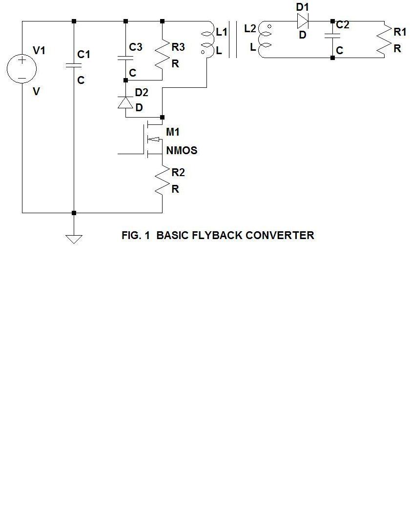
Fig. 1 shows the topology of a basic flyback converter (less the drive control and feedback circuits for simplicity.) This will be the basis for further discussion of key components and the basic function of the converter.

V1 is the source of voltage to be converted. If the source is an AC source it will have to be full wave rectified to DC before it is applied as the DC source to the converter. The full wave rectification circuit is not shown here for simplicity. C1 is the basic input filter capacitor. It must have a large enough value to filter noise from the switching of the transistor M1 and also be high enough to "hold up" the DC voltage to the converter in the event of a line droop. The time to hold-up the system is usually 1/2 AC cycles to 1 full AC cycle.

M1 is the main switching transistor that allows control of the duty cycle of the converter through the action of its control circuit (not shown.) R2 is used to sense peak current through the transistor and the current in the primary, L1, of the transformer consisting of L1 and L2.

R3, C3, and D2 work together to "snub" the peak voltage on the transistor M1 to help control the initial turn-off voltage spike which occurs on the drain of the transistor on each on-off cycle. R3 and C3 are carefully chosen to get the best snubbing without excessive dissipation in R3 or loss of energy being transferred to the secondary circuit.

L1 is the primary of the transformer and must be carefully designed to handle the sometimes high voltage input and the large peak currents that can be required. My previous post covers some of the design considerations for the primary.

The secondary circuit consisting of L2 of the transformer, D1, C2, and R1 should be isolated from the primary side of the circuit to protect uses from electrical shock from the voltage source which might be a high voltage. R1 represents the load which could be a combination of inductance, capacitance, and resistance. An Example would be an electric motor. One important note about C2 is that in flyback circuits, this capacitor has a very high ripple current with high peak values and it must be carefully selected for its current rating and long life. A good choice for this capacitor is the solid aluminum electrolytic capacitor or other long life types for low voltage outputs. Later posts will go into more detail on design of the secondary circuit.

Sunday, July 4, 2010

CALCULATING THE PRIMARY WINDING AND AIR GAP FOR A SWITCHMODE TRANSFORMER

In the previous blog we showed how to calculate the inductance needed for an example power supply with a max input of 1000 volts and a power rating of 150 watts. Now lets see how to calculate the number of turns required. This is the standard formula for a square wave voltage so it approximates the switchmode condition. This formula will give us a starting point and it also verifies that we have at least the number of turns to withstand the applied voltage without magnetic saturation:

N = Vpk * 10^8 / (4 * Bmax * Ac * F)

where N is the number of turns, Bmax is the maximum allowed flux density without saturation for the material to be used ( some type of ferrite ), Ac is the core area, and the frequency F. We will work in CGS units and the flux density will be in Gauss units.

For a 150 watt transformer, from experience I will estimate the size of the transformer as a cube approximately 5 cm on a side ( about 2 inches.) This will also be the approximate size of a magnetic structure of say an EI or EE structure. Assume that the structure will be an EE form with a single air gap in the center of the structure. With this size and form I will further estimate (based on experience that the core area will be a square cross-section 1 cm on a side or 1 sq. cm. Assume further that the operating frequency will be 100KHZ. Now we can calculate our initial number of turns from our equation above using Bmax as 4000 (you will need to check what Bmax is for the ferrite material you plan to use) as

N = 1000 *10^8 / (4 * 4000 * 1 * 100000) = 62.5 round off to 63

Now we will need to know what is the magnetic path length of the core structure we have selected. You will most likely use the number you find in the manufactures catalog. Here we will estimate it to be 10 cm based on the size of the magnetic structure and its form. Also we will use 1/2 of the Bmax value as our max operating flux level, or 2000 Gauss. Then we will use our data so far and the following formula to calculate the effective permeability of the core as

Ue = B * Pl / ( 1.257 * N * I )

We will use 1 amp as our max current I, flux density B of 2000 Gauss and for the magnetic path length Pl our estimate of 10 cm:

Ue = 2000 * 10 / ( 1.257 * 63 * 1 ) = 252.55 round off to 253

From the catalog we need to obtain the permeability, U, of the ferrite material we are going to use. Lets assume that the basic permeability is 2500. Now we can make a first calculation of the air gap from the formula

Lg = Pl * ( 1 / Ue ) - Pl * ( 1 / U)

Lg = 10 * ( 1 / 253 ) - 10 * ( 1 / 2500 ) = 0.0355 cm

The above would be enough calculations to build an experimental transformer, but it might be wise to do some more calculations to verify the previous results. I will not do all of the numerical examples here but I will show the equations you can use , still working in CGS units.

Re-calculate the number of turns based on the effective permeability, Ue, and the required current I :

N = B * Pl / ( 1.257 * Ue * I ) = 62.89

This value of 62.89 checks well with our original calculation of 62.5, so we will stay with 63 turns for the primary of the transformer.

Next we can calculate the actual inductance of our transformer primary for our design to this point:

L = 1.257 * Ue * N^2 * Ac * 10^-8 / Pl = 0.00126 Henry

This value is less than what we originally decided we needed (from the previous post) of 0.005 H. So we will need to increase the area of the core by a factor of approximately 4 increasing Ac to 4 cm sq.

Now we need to check on the core area, Ac, that we need so we will compute it from the desired inductance value and effective permeability, assuming we did not change it:

Ac = L * Pl * 10^8 / ( 1.257 * Ue * N^2 ) = 3.96 cm^2

The result of the calculation is obvious from looking at the equation. We could have also increased Ue or N to achieve the same result, but it is better to increase Ac so that the maximum operating magnetic flux is not increased. Now it would be good to run back through our above calculations with our new value for L and Ac to get a design closer to what is needed (several iterations may be needed.)

But lets look at a little more design work. It may be better to compromise between the original estimate of Ac and the new, so that you might want to try some new values for Ac and N. One thing to note in the inductance formula is that L is proportional to the square of N so we can just do a minor increase in N along with a more practical value for Ac to get the 5 mH inductance we want. To do this we will "push" the design a little making it a little more risky but easier to make the transformer. For example, as a more practical value lets try 2 cm sq.for Ac. Also lets increase the turns N by a factor of about 1.4 or to 90 turns. We can wind the primary as two layers of 45 turns each. After re-doing the inductance and operating flux density calculations we have the following (the reader should be able to do these calculations now):

V = 1000 volts (spec.)
I = 1.0 amps (spec.)
Ac = 2 cm sq. (changed)
N= 90 turns (changed)
Ue = 253 (did not change this)

L = 0.00515 mH
B = 2862 Gauss

So now the changes yield the inductance you want at the price of increasing the operating flux density but still staying considerably less than the maximum of 4000 Gauss. This would be a possible starting point to for your design, but you will still need to determine how to design the secondary windings. We will cover this in another post.

Friday, July 2, 2010

HOW DO YOU PICK INDUCTANCE FOR A FLYBACK CONVERTER?

In the initial design phase of a flyback converter, there is the usual need to pick or design the inductor-transformer as a basic component. So what should the primary inductance be set to? Well it depends on what the global specifications are for your power supply, i.e., maximum input voltage, power required at the output, and an estimate of the switching frequency of the power supply.

The switching frequency is usually decided on the basis of the design and manufacturing technology you have available to you and is usually between 100KHZ and 1MHZ. The higher the frequency is, the smaller the filter components need to be, but the more difficult the design and manufacturing gets to be. For example, if you already know that all of the power supplies you have designed or your company designs run at approximately 100KHZ, you will probably need to operate at that frequency.

So lets say that you have the following global specifications as a minimum to start with:

maximum input voltage 1000 volts.
minimum input voltage 600 volts.
power output 100 watts.
efficiency 70% minimum

So now it is easy to compute the input power, Pin, based on the output power, Pout, required and the efficiency, e :

Pin = Pout / e = 100 / 0.7 = 143 watts

To provide a little power safety margin, lets round up to 150 watts for the required input power.

We will assume for this initial calculation that load current is reasonably constant so that we can compute the average input current that is required at the maximum input voltage, Vinmax, as

Iavg = Pin / Vinmax = 150 / 1000 = 150 ma

Lets assume further that your converter will operate at a frequency F = 100KHZ

Now my rule-of-thumb formula for the required inductance L is the following:

L = Vinmax * Dmax * T / Ipk where Dmax is the duty cycle, T is the switching period, and Ipk is the peak switch corresponding to the max duty cycle (from the equation V = L * di / dt .) Note that Ipk will never be zero in theory or in real operation.

We can re-write the equation for L in terms of frequency as

L = V * D / ( Ipk * F )

Assume that we will allow an Ipk of 1 amp before the switch is turned off. At a duty cycle of 0.25 we would have an average current input of approximately 250 ma which would allow a peak power of 250 watts input at 1000V input (0.25 * 1000) and 150 watts at 600V minimum input. This should be plenty of power capability. If the minimum input voltage is lower, more peak switch current will have to be allowed, Ipk.

Assume worst case conditions for the inductor; maximum input voltage and maximum duty cycle of 50%. Compute the required inductance at 100KHZ switching frequency:

L = Vpk * D / (Ipk * F) = 1000 * 0.5 / ( 1 * 100000 ) = 0.005 Henry = 5 mH

Now the next thing you need to consider is the fact that the inductor-transformer must not be allowed to saturate due to excessive magnetic field density in the core. If it does saturate the inductance will drop to a very low value and current will become an indefinitely large value possibly destroying the power supply.

The equation for calculating the maximum flux density ( and verifying that the value is within the inductor-transformer specifications ) is as follows:

Bmax = Vpk * 10^8 / ( 4 * N * Ac * F )

where N is the specified number of primary side turns and Ac is the core area. The above equation is a worst case situation where any air gap is very small or zero. Note that the allowed Bmax depends on the magnetic material in the core which is usually a ferrite material.

Saturday, December 29, 2007

Mutiphase Buck Converters


My notebook drawing above shows what might be a typical multiphase buck converter as a simplified block diagram of what a 3-phase system might be like (I don't claim to have inverted this.) The basic elements are a master control IC, slave gate drivers 1, 2, 3, and mosfet switches Q1-Q6. In a real implementation, the mosfet switches and gate drivers might be combined into one IC. One example similar to my drawing is the International Rectifier (TM) part iP2001. The main control IC usually has the basic functions of PWM signal generation, current and voltage sensing, frequency compensation, and some type of control bus which could be simply a set of external switches set to pull certain control bits up or down, an external microprocessor, or a serial bus such as an IC square (TM) or combinations of control methods. Each set of gate driver and pair of mosfets act like a separate high frequency synchronous buck converter as described in my previous article.
The three buck converters are paralleled into one system to form the 3-phase converter. Each phase operates in sync with the other phases at say 500KHZ each so the effective switching frequency is 1.5MHZ. Current is balanced in each phase by sensing the current in each inductor through the resistors R1, R2, and R3. Sometimes the current is determined by sensing the voltage drops across the upper mosfet in each pair, or by sensing the average current through the inductor. Inductors L1, L2, and L3 can be coupled for lower noise output. A complete description of the theory of coupling for lower noise is beyond the scope of the present article. Capacitors C1, C2, C3 represent possibly many capacitors in parallel that serve to filter noise and stabilize the converter. The inductance value, L1, for example and the effective capacitance C as the sum of all the capacitors set the pole and bandwidth of the converter as 1/(2*Pi*sqrt(L*C)) before compensation. The compensation network might be similar to the resistor-capacitor network shown between pins VSENS, FB, and COMP. Typical operating conditions could be a 12V input (Vi) and a 1.1 to 2V output at high currents. The 3-phase converter shown above could be capable of 60 amps output or more depending on the component ratings. The author designed and tested a 4-phase converter capable of 100 amps output at 1.2 volts with less than 15mv peak-to-peak noise. The typical application would be to power a low voltage microprocessor, graphics processor, or other processors that require large currents with high speed current demand pulses with low noise.

Monday, December 3, 2007

What is a Synchronous Buck Converter?


Fig. 1 shows a simplified synchronous buck converter circuit. U1 is what is called a “synchronous buck controller” because of its capability to control the power switches Q1 and Q2 in a synchronous fashion using its gate drive output labeled HG and LG in Fig. 1. The controller may have additional functions not shown in Fig. 1, such as a “boot” voltage input to be able to drive Q1’s gate with a drive voltage signal above the input power rail to insure that the switch will turn on. The boot voltage may be derived from the switching node S1 or from a VCC supply voltage that is sufficiently higher than the power rail voltage.

U1 may also have a way of sensing current into S1 or through the high side mosfet Q1 or through the inductor L. Sometimes the voltage drop across Q1 is used to monitor current. The circuit may then be operated in current mode control (see my previously posted article for a description of current mode control.)

The circuit is called synchronous because the top switch is turned on when the bottom switch is turned off and vice versa. This eliminates the power loss in a diode that would otherwise need to be used in place of Q1. Of course, there cannot be any significant overlap of the on-times of Q1 and Q2 or there will be what is called “cross-conduction” which will cause heating, power loss, and possible failure of the switches due to over-current. On the other hand, there should not be too much dead time or a large Q1 turn-off voltage spike will occur at the open end of the inductor possibly causing switch failure or damage to U1.

The LC filter removes noise and ripple voltage from the output. R1 and R2 adjust the feedback voltage level to be compatible with the internal voltage reference included in U1. R3, R4, and C2 form a typical feedback compensation network. Note that the equivalent series resistance (ESR) of the filter capacitor C is important in determining the compensation network, and of course also affects the amount of noise that is seen at the output. ( See also my first article posted for the main equations governing the buck circuit.)

Saturday, December 1, 2007

What is current mode control?


How does current mode control work? Referring to Fig. 1, the block SW represents the power switching stage of a PWM converter (see previously posted article.) HC is the inner current control loop which converts the sensed current into a voltage signal that represents the magnitude of each current pulse generated by the switching stage. In this way we can achieve pulse-by-pulse current control. Pulse-by-pulse control allows very rapid response to over-current or fault conditions. The current sensed is usually the current ramp that enters and energizes the inductor. This energy will later be dumped into the filter capacitor C which filters output voltage ripple. The LC filter generates two poles in the transfer function which need to be dealt with by the feedback control and compensation system. One of the advantages of the current control method is that it tends to nullify one of the inductor poles so that the outside voltage control loop can have simplified compensation for the error amplifier A (see the URL listed below for more information on operational amplifiers and feedback.)

The outer voltage control loop senses a ratio of the output voltage, using the voltage divider R1 and R2. This voltage is compared to the voltage reference applied as one of the inputs to the error amplifier. The error amplifier may have compensation elements Z1 and Z2 in Fig. 1, but with the current mode control inner loop, the compensation can usually be simplified to a simple RC net for Z2 and just a resistor for Z1. The output of the voltage error amplifier is summed together with the current sense signal to control the operation of the converter. The two control loops provide excellent control of the system when properly designed.

One caution is that for higher duty cycles, a sub-harmonic or low frequency oscillation may occur. Fortunately there is a cure for this problem called slope compensation that adds some slope to the current sense ramp to prevent the instability. Excellent articles on this subject are provided by Venable ™, Ridley Engineering ™, and Texas Instruments ™.

There are also good current mode control integrated circuits that combine circuits for both the current mode control and voltage mode control loops. These IC’s are available from Texas Instruments ™, Linear Technology ™, and other companies. You may want to look-up the datasheet for an IC made by Texas Instruments ™ by the part number UC1842. This family of IC’s is the grand-daddy of current mode control IC’s and is still available. It also available from a number of manufacturers and distributors.

Thursday, November 29, 2007

What is Pulse Width Modulation?


How does pulse width modulation work? Referring to Fig. 1, the classical method of voltage mode PWM is to compare an error signal to a reference ramp oscillator waveform as shown in Fig. 1. In the figure, as the error signal crosses the rising edge of the ramp, the comparator output goes to its high output level, and conversely when the error signal crosses the falling edge of the ramp, the comparator switches to its low level output.

Also, if we wish the duty cycle to increase when the error signal falls, to correct the system output, or increase system output, such as the voltage of a regulated converter, or the speed of a motor, for example, the example of Fig. 1 shows exactly that effect. As the error signal drops, the pulse width increases, thereby applying more power, or voltage, or more signal level to the load.

Why do we convert the error signal to a PWM signal? Because the PWM signal can operate an electronic switch such as a mosfet or a transistor that will rapidly switch on and off and transfer power more efficiently. The comparator output, if it is 0 to 5 volts or higher, can drive the gate of a power mosfet directly thereby controlling a lot of power with a small signal. If needed, the output signal of the comparator can be buffered with a high current buffer pulse amplifier to allow the ability to drive very large transistor switches and even paralleled transistor switches for high power.

Wednesday, November 28, 2007

The Basic Buck Converter


A simple single switch buck converter is shown in Fig. 1. Because of the power loss in the diode D1, the single switch buck converter is not suitable for high current or high power applications. It would work, however, with suitable choice of components, for low power, low current, and low voltage applications. If the input voltage is less than 40 volts, D1 could be a Schottky diode to improve efficiency. Not shown in Fig. 1 is the method of developing the high frequency pulse drive signal which is usually a type of pulse width modulated (PWM) signal that drives Q1 either into a saturated-on condition of a fully turned off condition. As long as Q1 is either in the full on or full off state, alternately at the converter switching frequency, the power dissipation in Q1 will be relatively low as power is dissipated only during the times that current is flowing through the switch when voltage across the switch is not close to zero. There are some other losses in Q1 which are also present which we will discuss in another article.

We can define the duty cycle D at any given time as the ratio of the time the switch is on to the total time of the each switching cycle (also called the switching period.)

D = Ton / Tsw

The switching frequency can be constant or variable, but it is usually relatively constant under steady state conditions can be calculated as

Fsw = 1 / Tsw

The output voltage is set by the duty cycle and the input voltage under steady state conditions as

Vout = D*Vin = Vin * Ton / Tsw

The maximum or peak voltage, Vds, across the mosfet Q1, drain to source is

Vds = Vin + Vd

where Vd is the forward voltage of the diode. The function of the diode is to allow current to continue flowing to the load when Q1 is in the off state. The peak Q1 drain current is

Idrain = I_load + dIp_inductor / 2

where dIp_inductor is the peak inductor current above the DC load current and can be calculated as

dIp_inductor = Vin * Ton /L

where L is the inductance value in Henries. We note here that the capacitor C1 has to be rated to handle the ripple current from the inductor, and of course be rated for the output output voltage. If C1 is a tantalum capacitor, it is usually de-rated by 50% for the output voltage of the converter.

Finally, the diode average current can be computed as

Id = I_load*(1-D)

The diode has to be rated to handle the input voltage and its average current.

We have now covered the basic calculations for the single switch buck converter which would allow a power stage to be designed with selection of components for the application. We should also note that the buck converter is used only to reduce some input or bus DC voltage down to a lower DC voltage. We have not yet covered drive signal generation (PWM) for Q1 gate drive, nor the control network which is usually a feedback loop with frequency compensation elements.